
How AI Chips Are Made
Adapted from a section of a report by Erich Grunewald and Christopher Phenicie, this blog post introduces the core concepts and background information needed to understand the AI chip-making process.
Over the past decade, advances in AI have been driven by the use of more and more sophisticated AI hardware. Many modern AI systems, like chatbots such as OpenAI’s ChatGPT and Google’s Gemini, are based on deep learning models trained and deployed using thousands of specialized AI chips housed in data centers. An analysis by Epoch AI suggests that an estimated 40% of the growth in training compute has been due to using larger numbers of chips, with the remainder being split between using higher-performance AI chips (~27%) and training models for longer durations (~33%).
As a result of these trends, there are now major efforts underway to produce unprecedented quantities of AI chips. As an example, while OpenAI’s GPT-3 model released in 2020 was trained with an estimated 10,000 NVIDIA V100 chips, its GPT-4 model released in 2023 was reportedly trained with 25,000 NVIDIA A100s, and it is planning even larger supercomputers, e.g., one in collaboration with Oracle using 400,000 of NVIDIA’s new GB200 chips. With each generation, these chips get better and pricier – according to one study, the computational performance of AI chips doubles every 28 months. NVIDIA, which dominates the AI chip market with an estimated 80 to 95 percent share, shipped an estimated 1.5 to 2 million NVIDIA H100s in 2024 – the H100 being its most advanced chip that year – a threefold increase over 2023.¹
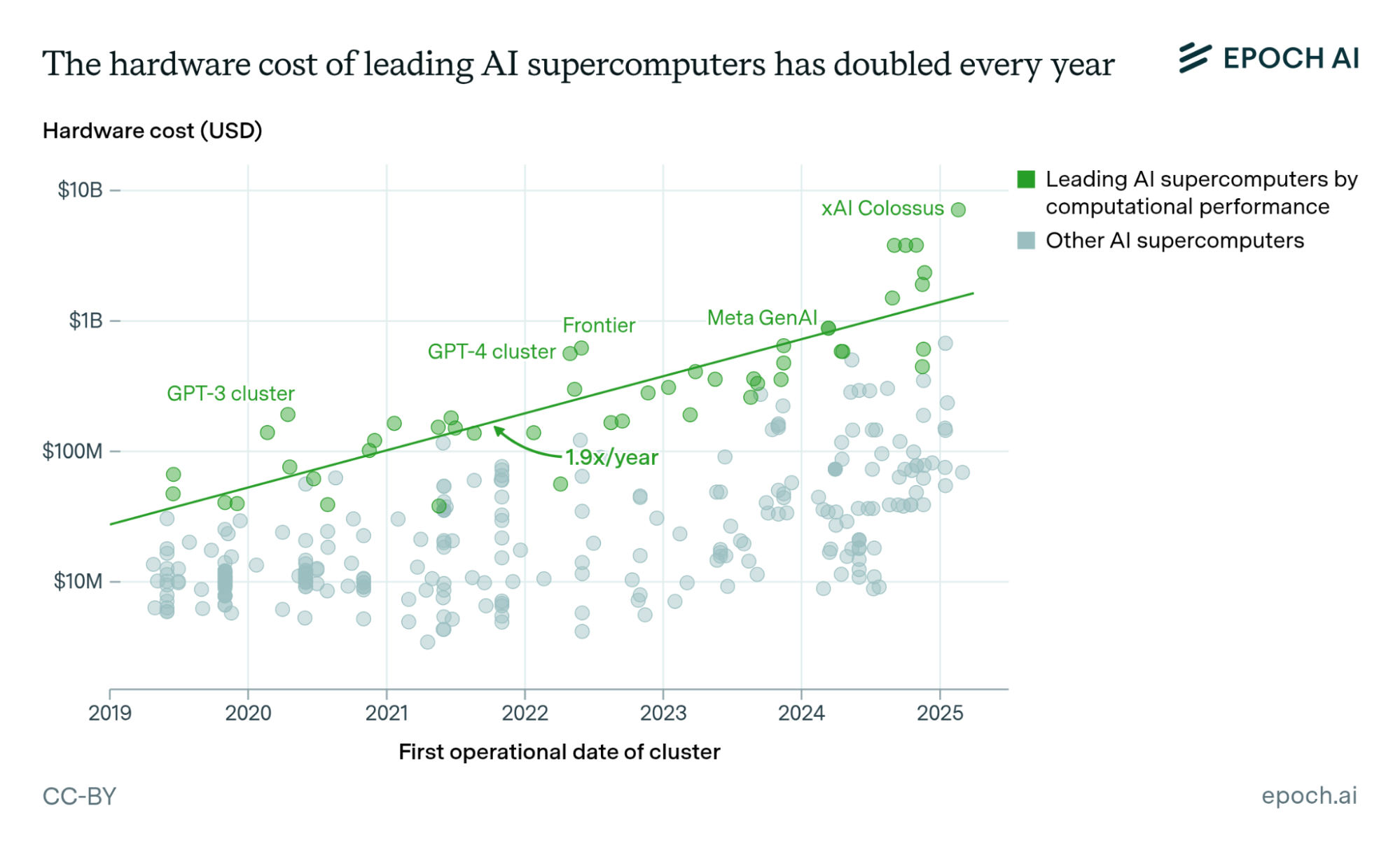
Figure 1. Firms are building increasingly large supercomputers, containing more, and more performant, AI chips.
But what is an AI chip? A chip (“integrated circuit”) is a group of electronic circuits laid out on a piece of semiconductor material. AI chips are integrated circuits specialized for AI training and/or deployment (“inference”) workloads. AI chips come in different types. Some, like Google’s Tensor Processing Units (TPUs), are application-specific integrated circuits (ASICs) – chips customized for highly specific workloads such as tensor² operations used in deep learning training/inference. Other AI chips, like those made by NVIDIA, are graphics processing units (GPUs) – chips designed to more generally execute mathematical operations in a highly parallel manner.³
At a high level, AI chips are made in three steps: design, fabrication, and packaging. After the chips are packaged, they are typically assembled into devices (“AI accelerators”), which in turn are integrated into servers that can be mounted in data center racks.⁴ The semiconductor design and manufacturing process is not only highly demanding and sophisticated but also fascinating. The remainder of this blog post provides an overview of that process.


Figure 2. Left, an NVIDIA H100 printed circuit board, without casing, with the GH100 GPU (outlined in red) and six surrounding high-bandwidth memory (HBM) chips (outlined in blue) in the center. (Note that, in practice, the H100’s SXM5 and PCIe Gen 5 form factors ship with five HBM stacks enabled, while the H100 NVL ships with six stacks.) Middle, an NVIDIA A100 accelerator with casing. Right, Jensen Huang, president and CEO of NVIDIA, signing the first delivered NVIDIA DGX server.
Design
Chip designers specify high-level requirements, turn those into a detailed abstract model of the circuit logic, and use electronic design automation (EDA) software to translate that model into a blueprint of the physical circuit. The high-level requirements are typically based on earlier research carried out to find novel ways of improving performance. The design process involves defining the structure (“microarchitecture”) of the circuit’s logic components, designing each component or licensing a ready-made component (“IP core”) from a vendor, and specifying the connections between components. It is an iterative process. A chip’s specifications can be revised to balance cost and performance trade-offs. The design is also tested and validated to help ensure it will behave as expected once fabricated, for example, by simulating the design, running checks on code to scan it for errors, and making formal proofs about parts of the circuit logic.
An AI chip is designed for a particular process node. The fabrication plant (“fab”) will provide the chip maker with a process design kit (PDK), which provides the necessary information to design and validate chips for one of the fab’s processes. The result of the design process is design files containing a detailed description of the chip’s physical layout, which is shared with the fab. Chip design is a difficult and laborious process. Chip designers like NVIDIA and AMD have tens of thousands of employees, and the design process for cutting-edge AI chips lasts for a year or longer.⁵
Fabrication
Material preparation
Chips are fabricated on thin, circular slices of semiconductor⁶ called wafers, typically 300 mm (12 inches) in diameter.⁷ The most common semiconductor used is silicon. Modern silicon wafers, which are grown in furnaces and then sliced, polished, cleaned, doped, and inspected, need to be extremely pure and smooth in order to avoid defects in chip fabrication.
(Avoiding defects is a priority because improved yield – the percentage of chips that are defect-free – directly translates to increased profitability. Defects – which can be caused by contaminants, environmental conditions, equipment issues, and more – are a problem in semiconductor manufacturing because it involves hundreds of sequential steps and extreme precision and environmental control.)
Prior to fabrication, photomasks are produced from the description of the physical layout provided by the chip designer. A photomask holds a pattern that will be imprinted onto the wafers, like a custom stencil.⁸ Photomasks are created using direct-write mask writers, involving multiple stages of optical or electron beam (e-beam) lithography, etching, and inspection to ensure that there are no defects.
In addition to wafers and photomasks, semiconductor manufacturing also requires various specialized chemicals and gases.
Wafer fabrication
Supplied with silicon wafers and photomasks, the fab is ready to manufacture the chips. The wafer fabrication process involves imprinting patterns onto the silicon wafer in layers of different materials, including insulators (dielectrics), conductors (metals), and semiconductors. It is a highly difficult and complex process, as it demands extreme precision, involves hundreds of individual steps, and must, at the same time, achieve high economic efficiency. What follows is a simplified description of that process.
First, the transistors and other devices (resistors, capacitors, etc.) are formed by repeatedly depositing, patterning, and etching layers of materials. The wafer is always processed as a whole, allowing trillions of transistors to be created in a short amount of time. The reason why the wafer can be processed in one go is patterning techniques. To form patterns, a light-sensitive chemical (“photoresist”) is deposited on top of a material and, using a photolithography machine, exposed to ultraviolet light passing through the photomask, then developed, leaving a pattern of gaps in the photoresist. (This is akin to how light reacts on photographic film in a camera.) The developed photoresist now acts as a mask, allowing the material underneath to be partially etched away, after which the photoresist is washed away, leaving behind only the patterned material. These steps are repeated until the devices are fully formed.
In this patterning process, it is also necessary to modify the electrical properties of parts of the semiconductor; to do this, specialized substances (“dopants”) are introduced using a technique called ion implantation. When excess material needs to be removed from the wafer’s surface, it is polished in a chemical slurry using a technique called chemical mechanical planarization (CMP). To remove contaminants and residue, the wafer is periodically cleaned using chemicals, plasmas, and a variety of physical techniques like sound waves or jets.
After the devices (transistors, etc.) have been formed, layers of metals and insulators are deposited and etched with chemicals to form connections between the devices. The steps used to create the metal layers resemble those used to form the devices underneath, as they also involve photolithography, deposition, etching, and planarization, and are also repeated with different patterns over multiple layers. Finally, a protective layer is deposited on top of the metal layers, with gaps etched in it for connections to external circuitry.
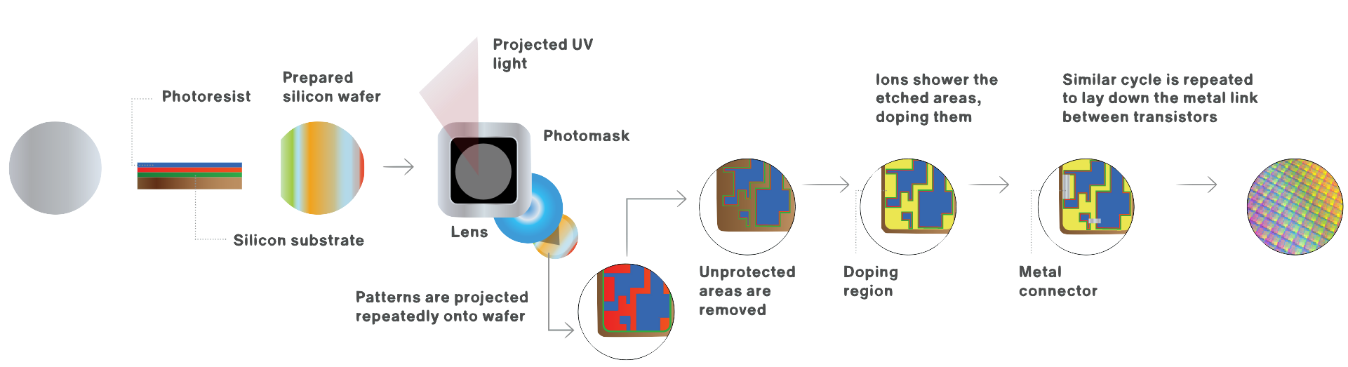
Figure 2. A simplified illustration of the wafer fabrication process.
The entire process is almost fully automated. Wafer handler tools transport and align wafers between and during process steps, and process control tools regularly monitor the wafers for defects, as detecting defects early on is critical to keeping costs down. However, human engineers and technicians still provide oversight, maintenance, and efficiency improvements.
Assembly, test, and packaging
After fabrication, the patterned wafers are typically sent to a different facility for assembly, test, and packaging (ATP).⁹ First, the silicon wafer is cut into individual, rectangular chips (“dies”). Those dies are then tested, and good dies are encased in a protective covering. Once packaged, the chips undergo final functional testing and “burn-in”, where they are tested at extreme temperatures and voltages. ATP is sometimes collectively referred to as “backend” manufacturing, with wafer fabrication being “frontend” manufacturing. Although the packaging process is less complex than the fabrication process, it is not trivial.
While the main purpose of packaging has traditionally been to protect the chip from corrosion and other damage and to add connectors for other chips, advanced packaging techniques are now an increasingly important driver of semiconductor progress. “Advanced packaging” refers to a group of techniques for arranging multiple fabricated chips and “chiplets” together in a single package. (A “chiplet” is a small chip designed to be combined with others in a package.) Two relevant variants of advanced packaging are 2.5D, where multiple chips are arranged on an “interposer” chip that facilitates communication, and 3D, where chips are stacked on top of each other. Such techniques include:
Through-silicon vias (TSVs), used to connect vertically stacked dies. TSV is used to create high-bandwidth memory, and therefore necessary for modern AI accelerators.
Chip-on-Wafer-on-Substrate (CoWoS), used to stack chiplets on wafers. TSMC uses CoWoS to make NVIDIA H100 chips by packaging the GPU alongside six high-bandwidth memory chiplets.
Embedded multi-die interconnect bridge (EMIB), used for die-to-die interconnect. This accomplishes similar goals to 2.5D techniques like CoWoS, but without requiring, or benefitting from, a large interposer, which is costly and consumes space.
Hybrid bonding, used to stack chips or wafers on wafers using direct copper-to-copper interconnects.
Combining multiple smaller chips in a single package can offer higher yield, reduce the maximum distance of connections, and allow for the heterogeneous fabrication of chiplets using different fabrication processes (e.g., using advanced, expensive nodes for high-value chiplets and cheaper nodes for other parts).
Conclusion
Making advanced AI chips involves one of the most complex manufacturing processes that has ever existed. Each step in the AI-chip-making process – from design to fabrication and ATP – impacts the performance, cost, and quantity of AI chips made. Understanding how AI chips are made can help policymakers, industry, and civil society develop good industrial and compute policy while also anticipating future AI developments.
Moreover, because they are so closely connected to AI progress, AI chips have emerged as a focus point of geopolitical competition, for example, having been the target of wide-ranging US-led export controls against China. Our Introduction to AI Chip Making in China report contains more detail on AI chip making, especially as it relates to Chinese efforts to develop better domestic AI chips.
End Notes
The market share estimate excludes Google Tensor Processing Units (TPUs) – another type of AI chip – as Google does not sell these chips, opting instead to rent them out from its own data centers.
You can think of a “tensor” as an array of a particular dimension, e.g., a scalar, a vector, or a matrix.
GPUs are so named because they were originally designed to perform computations needed to render graphics. Many GPUs, such as those in consumer-grade graphics cards, are still optimized for graphics rendering, but some GPUs are now primarily optimized to perform AI workloads (which have similarities with those in graphics rendering). Like TPUs, NVIDIA’s data center GPUs have features aimed at speeding up tensor operations used in deep learning, but in addition to those, and unlike TPUs, GPUs also have features unrelated to deep learning, such as for genomics and graph analysis.
Sometimes the AI chips, housed on printed circuit boards but without the casing of an accelerator, are mounted directly on motherboards. NVIDIA products of this sort are sometimes called “SXM modules”.
The claim about how long AI chip design takes is based on conversations with people familiar with the chip design process. In addition, according to Jouppi et al. (2021), it took 27 months between the deployments of TPUv1 and TPUv2, 15 months between TPUv2 and TPUv3, and 15 months between TPUv3 and TPUv4, though it is possible that the design processes overlap, or that there are pauses between them. Making a new chip design from scratch, rather than iterating on previous designs, is more involved and takes longer.
A “semiconductor” is a solid material that conducts a moderate amount of electricity – more than insulators (like rubber), and less than most metals (like copper). Sometimes “semiconductor” is also loosely used to refer to a chip made with a semiconductor material.
Other wafer sizes, such as 200 mm (8 inches) are also used, but advanced process nodes typically employ the larger 300 mm wafers, partly because the fixed costs of processing each wafer are higher for more advanced processes. Indeed, the trend over the last six decades has been one of increasingly large wafers being introduced for increasingly more advanced processes.
Unlike stencils, photomasks do not look exactly like the physical patterns they help print. That is because they must compensate for distortions caused by things like light diffraction, using techniques like optical proximity correction.
These vendors are grouped under the term outsourced semiconductor assembly and test (OSAT). Some chip manufacturers do carry out ATP in-house, at least for some of their chips.